

RF PCBs tested for reliability
Testing for reliability is an essential part of the design and production process for RF (Radio Frequency) PCBs (Printed Circuit Boards). Given that RF PCBs are used in high-performance applications such as telecommunications, radar, and wireless communication systems, their reliability is paramount to ensuring the proper functioning and longevity of these critical systems. RF PCBs are subjected to various tests to assess their durability, signal integrity, and performance under different operating conditions. In this article, we will explore the primary methods used to test RF PCBs for reliability, including thermal cycling, signal testing, environmental testing, and more.
One of the most important tests for RF PCBs is signal integrity testing. This type of testing ensures that the RF signals transmitted through the PCB remain accurate and free from distortion or interference. Since RF signals operate at high frequencies, even small imperfections in the PCB layout or material can lead to significant signal loss, reflection, or distortion. Signal integrity testing involves measuring the performance of the PCB’s transmission lines, ensuring that the impedance is consistent across the entire signal path, and verifying that there are no significant signal reflections. This is typically done using network analyzers, which measure parameters like return loss, insertion loss, and phase shift, providing a clear picture of how well the PCB is performing at the intended frequencies.
Another critical aspect of testing rf pcb for reliability is thermal testing. RF circuits generate heat during operation, and if this heat is not properly dissipated, it can lead to component failure or signal degradation. Thermal testing involves subjecting the PCB to varying temperature cycles to simulate real-world operating conditions. This can include both thermal shock testing, where the PCB is rapidly heated and cooled, and steady-state temperature testing, where the PCB is exposed to constant, elevated temperatures over an extended period. Thermal cycling tests help identify issues such as thermal expansion, solder joint fatigue, and material degradation, which can compromise the PCB’s reliability over time.
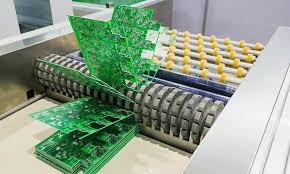
How are RF PCBs tested for reliability?
Environmental testing is another essential part of the reliability testing process for RF PCBs. RF systems often operate in harsh environments, such as outdoors or in aerospace and military applications, where they are exposed to moisture, dust, vibration, and other environmental factors. Environmental testing simulates these conditions to ensure the PCB can withstand these challenges without compromising performance. Common tests include humidity testing, where the PCB is exposed to high levels of moisture to see if it affects the PCB’s electrical performance, and vibration testing, where the PCB is subjected to mechanical vibrations to check for issues like cracked solder joints or delamination of layers. These tests are designed to simulate real-world stresses and ensure that the PCB can maintain its performance and durability under adverse conditions.
Reliability testing also includes high-frequency performance evaluation. RF PCBs must be able to handle signals at very high frequencies without excessive loss or distortion. To assess this, designers often perform tests that evaluate the PCB’s performance at different frequencies and power levels. These tests check for issues such as signal attenuation, cross-talk, or other electromagnetic interferences that could compromise the quality of the signal. In some cases, testing may be done using a vector network analyzer (VNA) to examine how the PCB behaves at various frequencies across the design’s bandwidth. This high-frequency testing ensures that the PCB can operate effectively in its intended application, whether it is in communications, radar, or other high-performance systems.
Electrical testing is also a crucial part of RF PCB reliability testing. This typically includes continuity tests, which ensure that all electrical connections on the PCB are intact, and impedance tests to verify that the signal traces maintain the correct impedance throughout the board. Automated Optical Inspection (AOI) is another technique used to detect manufacturing defects, such as misaligned components, soldering issues, or other physical defects that could affect the PCB’s reliability. These tests help identify problems before the PCB enters the field, preventing costly failures later in the product’s lifecycle.
Finally, life-cycle testing is used to evaluate how the PCB will perform over time. This may involve accelerated life tests, which simulate years of use in a shorter time frame by applying high levels of voltage, temperature, or vibration. This type of testing helps predict how the PCB will degrade over time and provides insights into its expected longevity, ensuring that the PCB will continue to perform reliably in real-world applications.


