

Typical Sizes of Blind Via Holes
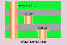
A via (pronounced “vy-ah”) is a connective, plated-through hole in a printed circuit board that routes a trace vertically from one layer to another. There are three different types of vias in a PCB: blind via, buried via, and through-hole via (PTH). Understanding what they are, how they’re used, and their standard sizes is an essential part of PCB design. Choosing the right via size can mean the difference between a successful design and a faulty one.
The typical sizes of blind via hole depend on a number of factors, including the stack-up structure and fabrication method of a specific PCB. They can also be a factor in the overall design requirements of a project. These include signal integrity, impedance control, and RF line termination.
While PTH vias are the norm in most PCB designs, there are occasions when it is necessary to use blind or buried vias. These are typically in high-density interconnect (HDI) applications where the amount of space available on the outer layers of a multilayer board is limited.
PCB vias are a critical component in many modern electronic devices, and they help ensure that the signals on the board are properly routed. They are also required in the construction of complex multi-layer printed circuit boards.
The Typical Sizes of Blind Via Holes
There are several ways to create a blind or buried via, and each one has its own unique advantages and disadvantages. The most common method is to drill them using a laser, which is relatively fast and inexpensive. However, this can cause the copper and dielectric layers to separate from each other, leading to a loss of electrical conductivity and other issues.
Another way to create a blind or buried via is to use a sequential lamination technique. This involves drilling a thin piece of laminate, then processing it for both the copper and the dielectric layers separately. The individual layers are then laminated together, creating a PCB with holes in all of the layers except for the surface layer. Then, the hole can be etched and plated before being laminated again with the other layers to form the final product.
Both blind and buried vias can improve the performance of a PCB by reducing noise, EMI, crosstalk, and other interference problems. They can also increase the reliability of the circuit by reducing the chance of cracking or delamination in the board. In order to maximize the benefits of these vias, it is important that they are completely filled with copper, and that the ratio between the diameter of a blind or buried via and its depth (the aspect ratio) is kept low.
In order to avoid these issues, it’s important to discuss the use of blind or buried vias with your PCB supplier before starting on the design. They will be able to help you determine the stack-up structure that is best for your project and will advise you on any special requirements or considerations, such as the size of an annular ring, that you may need to take into account.

