

Designing a Micro Via
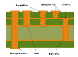
A micro via is a tiny hole in a printed circuit board that establishes electrical connections between the layers of the circuit board. The holes are drilled through the layers, then plated with copper, and they connect the various circuit board components with each other. There are several types of vias in PCBs – through-hole, blind, and buried, as well as stacked and staggered vias.
The process of designing a micro via starts with selecting the right copper foil thickness. The thickness influences conductivity, which in turn impacts reliability, and the choice needs to be carefully considered. Thicker copper foils can introduce issues during the manufacturing process, while thinner ones may not be able to disperse heat effectively enough.
Next, the designer needs to decide on a suitable laser drilling method. The process used can also impact the via’s quality, and a variety of processes are available for PCB manufacturers, including laser drilling, chemical etching, sputtering, and electroless copper plating.
The Process of Designing a Micro Via
Laser drilling is an ideal technique for creating microvias because it offers high precision and consistency and reduces the chance of flaws. It also ensures that the copper in the microvia is plated smoothly, which improves the strength and reliability of the connection.
Once the PCB layer has been etched, it must be cleaned to remove any residue. Then, the drilled holes must be filled with a conductive paste and plated over to provide continuity, resistance, and durability. To minimize the risk of failure, it is essential that the plated vias are subjected to rigorous testing and thermal cycling before they are deployed in an electronic product.
To prevent the formation of dimples, voids, bumps, and other structural defects in the plated copper, the vias must be inspected and polished. This is important because it helps to maintain the integrity of the microvias and ensures that they are a reliable link between the circuit board components.
A stacked microvia is simply multiple blind or buried microvias that are arranged in a stack and span between PCB layers. This is the standard way to form connections across multiple layers in an HDI PCB, and it allows designers to incorporate more complex structures that require higher interconnect densities. However, it is crucial that the design process enforces a strict upper limit on the via aspect ratio in order to avoid problems with reliability.
Stacked microvias are typically a combination of blind and buried vias, and the designers need to make sure that the internal buried microvias in the stack are filled with a sufficient amount of copper to ensure strong contact as they are deposited and plated by the manufacturer. To further increase reliability, the microvias should be staggered rather than stacked directly one atop another. This is because stacked microvias can be more susceptible to stress fracture around the barrel area when exposed to mechanical shock or thermal cycles. Staggered microvias are more resistant to these stresses, which is why they are preferred by many engineers.

