

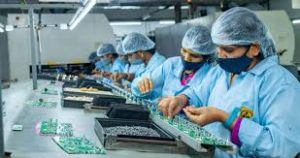
Pcb assembly services processes
Panelization, the process of grouping multiple PCBs onto a single larger panel, offers numerous benefits that optimize PCB (Printed Circuit Board) assembly services processes. By consolidating multiple PCBs onto a single panel, panelization streamlines various stages of the assembly process, including fabrication, assembly, testing, and handling. This approach improves efficiency, reduces costs, and enhances overall production scalability.
One of the key advantages of panelization is increased throughput during PCB fabrication. Fabricating multiple PCBs simultaneously on a single panel allows manufacturers to leverage economies of scale and maximize machine utilization. This results in shorter lead times and lower manufacturing costs per unit, making panelization an attractive option for high-volume production runs. Additionally, panelization minimizes material waste by utilizing the available space on the panel more efficiently, further reducing manufacturing costs and environmental impact.
Furthermore, panelization facilitates automated assembly processes, such as pick-and-place component placement and solder paste printing. Automated assembly equipment is designed to handle panelized pcb assembly services, allowing for simultaneous processing of multiple boards in a single operation. This significantly reduces cycle times and increases production throughput, enabling manufacturers to meet tight deadlines and customer demands more effectively. Additionally, automated assembly equipment can perform in-line quality control checks on panelized PCBs, ensuring consistency and reliability across all assembled boards.
How does panelization optimize Pcb assembly services processes?
Moreover, panelization simplifies handling and logistics throughout the assembly process. Panelized PCBs are easier to transport and store compared to individual boards, as they can be securely stacked and palletized for efficient handling. This minimizes the risk of damage or loss during transit and storage, ensuring that PCBs arrive at the assembly facility in optimal condition. Furthermore, panelization enables seamless integration with downstream processes, such as testing, inspection, and packaging, streamlining the entire assembly workflow and reducing overall lead times.
Additionally, panelization facilitates efficient testing and inspection of PCB assemblies. By grouping multiple boards onto a single panel, manufacturers can perform in-circuit testing, functional testing, and quality control inspections more cost-effectively. Testing equipment can simultaneously assess multiple boards on the panel, allowing for faster throughput and reduced testing costs per unit. Furthermore, panelization enables manufacturers to implement automated optical inspection (AOI) and X-ray inspection systems, which can quickly identify defects and ensure the quality and reliability of assembled PCBs.
Furthermore, panelization offers flexibility and scalability in PCB assembly services. Manufacturers can adjust the size and configuration of panels to accommodate different PCB designs, layouts, and production requirements. This scalability allows manufacturers to optimize production efficiency and resource utilization, regardless of batch size or product complexity. Additionally, panelization enables manufacturers to easily scale up or down production volumes in response to changing market demands, ensuring agility and competitiveness in dynamic industries.
In conclusion, panelization plays a crucial role in optimizing PCB assembly services processes by increasing throughput, reducing costs, improving handling and logistics, enhancing testing and inspection capabilities, and providing flexibility and scalability. By leveraging the benefits of panelization, manufacturers can streamline production workflows, improve efficiency, and deliver high-quality PCB assemblies that meet the stringent requirements of today’s electronics industry.


